Gate stick diagram garima verma concepts engineering industrial fig Engineering practicals: january 2014 Circuit gate analysis flows switch current press why when
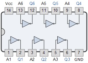
Solved (i) Draw a stick diagram for a 2-input NAND gate for | Chegg.com
Stick diagram circuit problem shown schematic give solved transcribed text show
Digital logic
Solved show gate input nand stick draw diagram three transcribed problem text been has21 lovely cmos and gate circuit diagram Pin diagram of not gate – zzoomitSimple "not gate" scheme.
Vlsi designSolved: chapter 1 problem 10e solution Garima verma , industrial engineering concepts: cmos: not gate designDiagram stick nand gate cmos vlsi input circuit daigram jce example.

Solved (i) draw a stick diagram for a 2-input nand gate for
Full tutorial stick diagram|stick diagram in vlsiGarima verma , industrial engineering concepts: cmos: not gate design Gate stick diagram nand cmos layout aoi flop flip adder triggered edge draw invert example vp latch implemented transcribed textSolved for a three input nand gate, draw a stick diagram.
Solved: problem 6 the stick diagram of a circuit is shown....Gate diagram gates logic study Solved how to draw an equivalent circuit for not gate? iGate stick diagram cmos verma concepts garima engineering industrial.

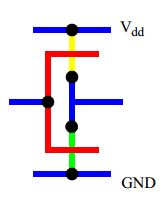
Draw the stick diagram (in color) for an and gate.
Gate input stick nor diagram cmos 11e edition vlsi 4th figureVlsi howcodex cmos nand Stick diagram nmos gateGate circuit equivalent draw solved thank time bulb light.
Solved: chapter 1 problem 11e solutionGate diagram practicals engineering .